The Helios Nanolab 600 has an ElstarTM electron column and a SidewinderTM ion column. In addition, it is equipped with an Omniprobe lift out system for TEM sample preparation. Lamellas prepared by FIB (Auto TEM software) can be transferred to a TEM grid for further thinning of the lamella. The Helios Nanolab 600 is also equipped with a cryo system and a cryo transfer chamber (Quorum) for fast freezing of samples and transfer into the specimen chamber. FIB milling as well as SEM imaging can be performed under cryogenic conditions. In combination with FIB, the cryo system provides an alternative to micro tomography regarding to preparation of facets.
In addition, the NanoBuilderTM software module allows rapid prototyping of complex structures using electron and ion beam induced deposition or gas-assisted etching processes.
Technical specifications
| Ion optics (Sidewinder™ column) Liquid Ga ion source FIB Res. 5 nm (@ 30 kV) | Field emission SEM SEM (Schottky field emitter) Res. 0.9 nm @ 15 kV | |
| Piezo-controlled stage x,y: 150 mm, z: 10 mm 6 inch wafer holder | Detectors CDEM, ETD, TLD | |
| Beam Chemistry Pt deposition Insulator Enhanced etch, IEE (XeF2) Selective Carbon Mill, SCE |
Omniprobe |
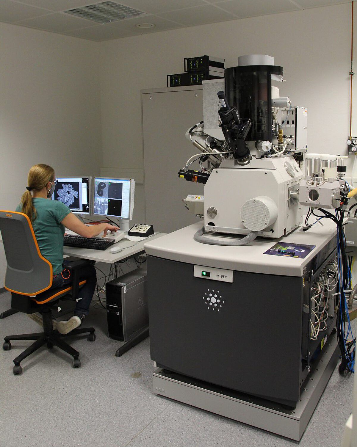
Helios Nanolab 600 im FIB Center UUlm
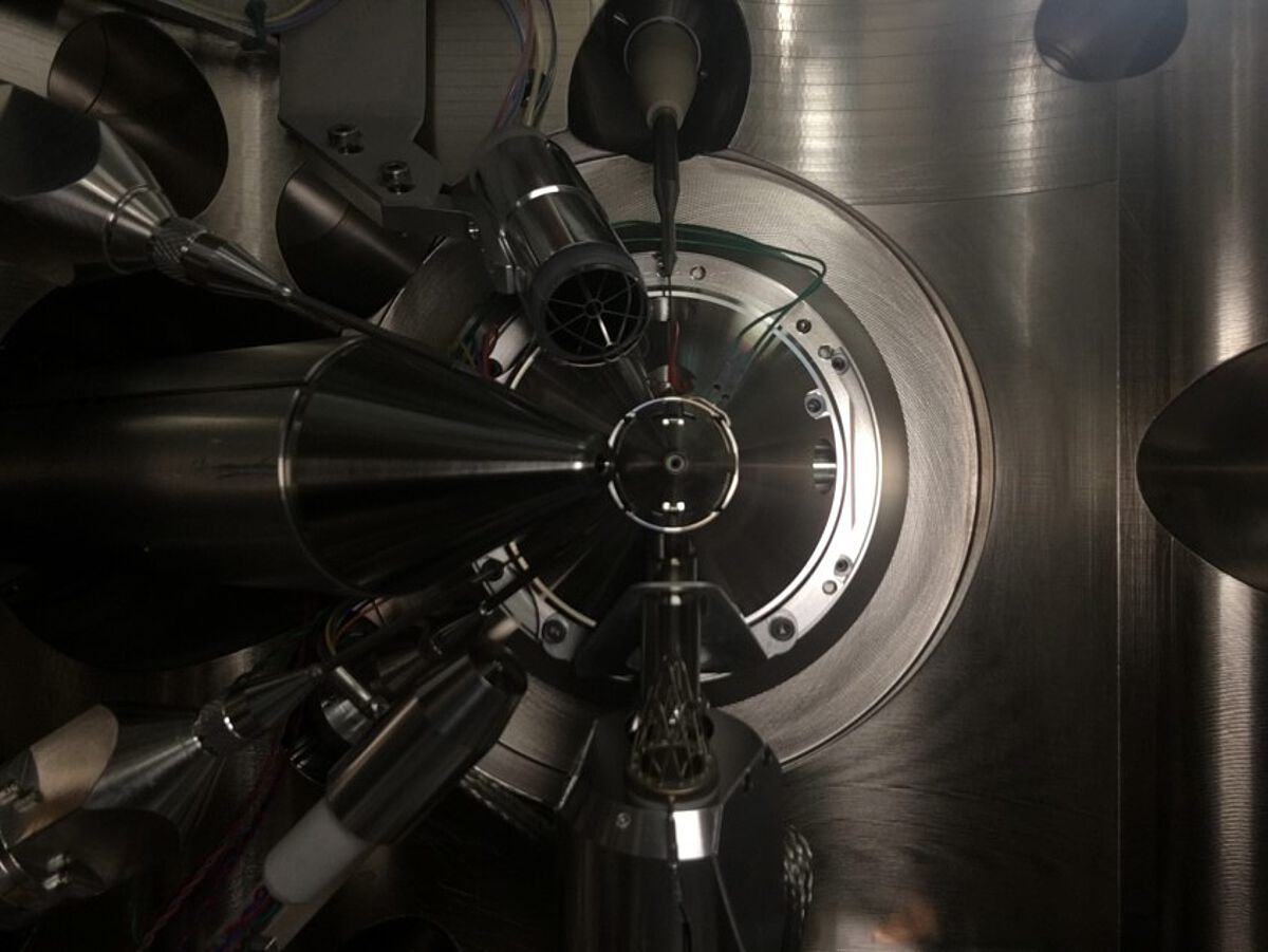
Innenansicht des Mikroskops
The Quanta 3D FEG is equipped with a state of the art SDD Apollo XV EDX detector (EDAX) for fast and precise qualitative and quantitative chemical analysis, and therefore more focused on analysis of materials. A DigiView 4 EBSD detector (EDAX) enables crystallographic investigations of specimens concerning grain orientations and textures.
In addition, the Quanta 3D FEG can be operated in ESEM mode. In this configuration the SEM is operated at a significant higher pressure (up to 4000 Pa) using water vapor to raise the pressure to the desired level. The water molecules remove charges built up by the electron beam allowing the investigation of non-conducting specimen without coating. ESEM mode can be used in combination with EDX and EBSD detectors. The ESEM mode can be used to investigate “wet” specimen.
Technical specifications
| Ion optics Liquid Ga ion source FIB Res. 7 nm (@ 30 kV) | Field emission SEM SEM (Schottky field emitter) Three imaging modes: | |
| Beam current 1.5 pA -65 nA in 15 steps | - high vacuum - low vacuum - Environmental SEM (ESEM™) | |
| Stage x,y: 50 mm, z: 25 mm | High vacuum: 1.2 nm at 30 kV (SE) Low vacuum: 1.5 nm at 30 kV (SE) ESEM: 1.5 nm at 30 kV (SE) | |
| Detectors ETD, GSED (ESEM Mode) EDX, EBSD | Beam Chemistry Pt, SiO2 deposition Insulator Enhanced etch (IEE) XeF2 Auto Slice and View™ |
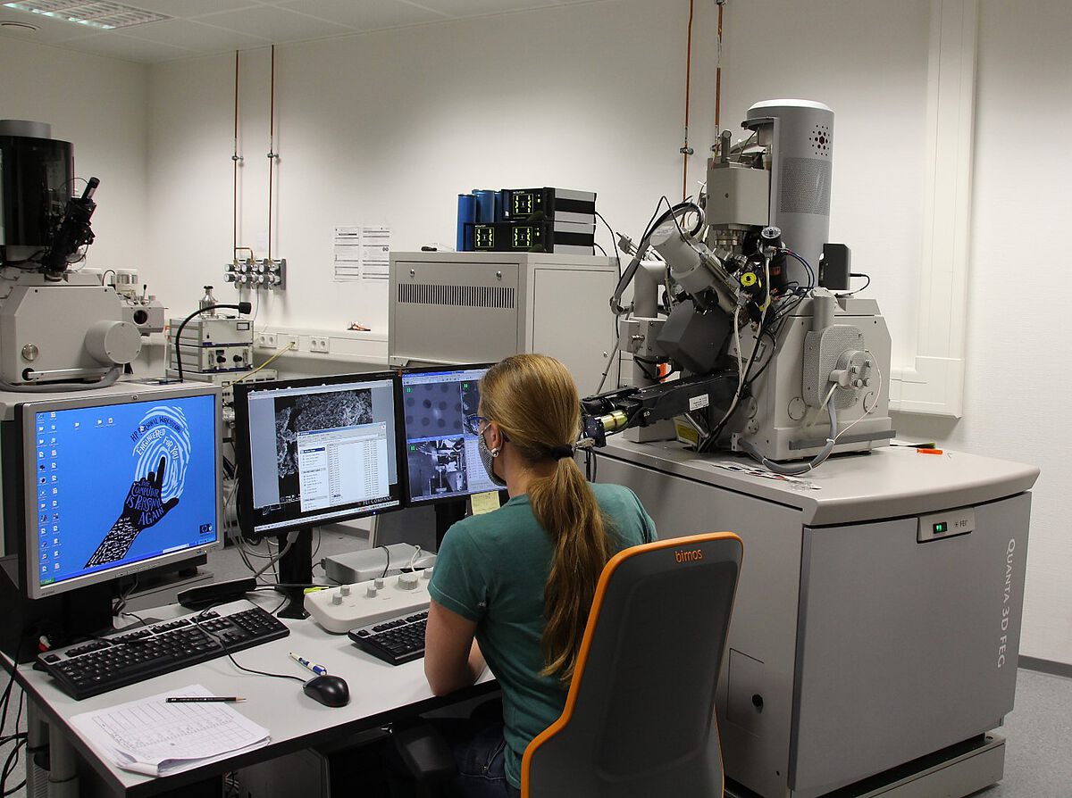
Quanta 3D FEG im FIB Center UUlm