Contributors
T. Lehnert, Y. Li, R. Leiter, J. Köster, U. Kaiser
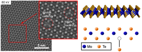
In high-resolution transmission electron microscopy (HRTEM), highly energetic electrons are used for imaging, which transfer appreciable amount of energy to the sample. This interaction leads to knock-on damage, if the transferred energy surpasses the binding energy, thereby displacing the nucleus from its position within the object. In addition, also electron-electron interactions like radiolysis or ionization, produce defects in the structures. Additional damaging mechanisms are sample heating, charging and chemical etching. Furthermore, the higher the electron dose rate the faster the defects are generated.
In our group, we try to find ways to increase the lifetime of samples under the electron beam. There are different approaches to counteract radiation damage. One way is to decrease the dose rates which results in a decreased signal-to-noise ratio. Increased resistance can also be achieved by encapsulating the sample with graphene. The resistance of the material in a so-called graphene heterostructure can be increased up to a factor of 600 [4, 6]. The third way is to find for each sample the optimal acceleration voltage in the TEM because at high voltages knock-on damage has a strong influence on damage and at low voltages, damage mechanisms like radiolysis and ionization predominate. Thus, the optimal acceleration voltage is slightly below the knock-on threshold and differs from material to material [3].
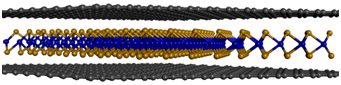
Besides reducing radiation damage, we are interested in defects and dopants that modify the properties like mass density, charge carrier concentration and thermoelectric conductivity [5]. For example, graphene which is a good electrical conductor can be turned into a semiconducting membrane if the transferred electron energies surpass the displacement thresholds [1].
[1] Kotakoski, J.; Krasheninnikov, A. V.; Kaiser, U.; Meyer, J. C. From Point Defects in Graphene to Two-Dimensional Amorphous Carbon. Phys. Rev. Lett., 2011, 106, 105505
[2] Kurasch, S.; Kotakoski, J.; Lehtinen, O.; Skákálová, V.; Smet, J.; Krill, C. E.; Krasheninnikov, A. V.; Kaiser, U. Atom-by-Atom Observation of Grain Boundary Migration in Graphene. Nano Lett., 2012, 12, 3168-3173
[3] Komsa, H.-P.; Kotakoski, J.; Kurasch, S.; Lehtinen, O.; Kaiser, U.; Krasheninnikov, A. V. Two-dimensional metal dichalcogenides under electron irradiation: defect production and doping. Phys. Rev. Lett., 2012, 109, 035503
[4] Algara-Siller, G.; Kurasch, S.; Sedighi M.; Lehtinen, O.; Kaiser, U. The pristine atomic structure of MoS2 monolayer protected from electron radiation damage by graphene. Appl. Phys. Lett., 2013, 103, 203107
[5] Lehtinen, O.; Komsa, H.-P.; Pulkin, A.; Whitwick, M. B.; Chen, M.-W.; Lehnert, T.; Mohn, M. J.; Yazyev, O. V.; Kis, A.; Kaiser, U.; Krasheninnikov, A. V. Atomic Scale Microstructure and Properties of Se-Deficient Two-Dimensional MoSe2. ACS Nano; 2015, 9, 3274-3283
[6] Lehnert, T.; Lehtinen, O.; Algara-Siller, G.; Kaiser, U. Electron radiation damage mechanisms in 2D MoSe2. Appl. Phys. Lett., 2017, 110, 033106
T. Lehnert, Y. Li, R. Leiter, J. Köster, U. Kaiser
Dr. Arkady Krasheninnikov (HZDR, Dresden)
DFG and MWK Baden-Württemberg in the frame of the SALVE project